
About
The group focuses on the development of smart sensors for the detection of atmospheric pollutant gases like COx, NOx, SOx, H2S, NH3 etc. and electromagnetic radiations based on thin film/nanostructures of metal oxides, III-nitrides, 2D materials, etc. The group is equipped with various thin film growth systems and thin film and sensor characterization facilities. Prototype metal-oxide based sensing device for CO gas has been designed and fabricated on alumina substrate with integrated platinum hot plate. Highly responsive UV photo-sensors have been developed based on III-nitride epitaxial layers and nanostructures.
Research Areas
Development of sensor devices for the detection of hazardous gases and electromagnetic radiations.
Metrology
Testing, validation and certification of the commercially available portable gas sensor devices are required in order to ensure reliable measurements. CSIR-NPL being the national measurement institute (NMI), we are in the process of creating a National facility for testing and certification of solid-state gas sensors following ISO 17025:2017.
Current R&D Projects
- Development of solid-state gas sensors for pollutant gases (In-house)
- Establishment of testing and calibration facility for portable gas sensors (In-house)
Major Research Highlights
- Prototype metal-oxide based sensing device for CO gas has been designed and fabricated on alumina substrate with integrated platinum hot plate.
- Highly responsive UV photo-sensors have been developed based on III-nitride based epitaxial layers and nanostructures.
Facilities
Growth & Characterization Facilities
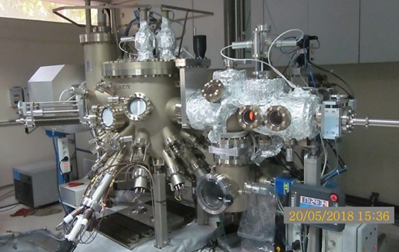
Plasma Assisted Molecular Beam Epitaxy (PAMBE):
The Riber Compact 21 PAMBE system shown in Figure is used to grow highly quality and extremely crystalline III-Nitride materials and provide precise control over the growth parameters. The highest quality material and highest reliability are key criteria in the design and manufacture of the system. It consists of three UHV chambers namely: Load-lock chamber (to load/unload the 6-platen cassette carrying wafers into the system), Buffer chamber (to store and outgas the wafers) & Growth chamber (to perform the epitaxial growth of compound semiconductor materials). Other main parts of the system include a number of pumps and gate valves (to achieve and maintain ultra-high vacuum), a lift (to move cassette vertically between load-lock and buffer chamber) and a magnetic transfer arm (to transfer the platen between buffer and growth chamber). The main growth chamber is a vertical UHV reactor equipped with standard effusion cells, (to supply ultrapure III group materials and dopants), a rf–plasma source (ADDON) to supply active nitrogen (N*) species, a Reflection High Energy Electron Diffraction (RHEED) gun (to real time monitor the growth of crystalline layers during the growth processes), a residual gas analyser (RGA), a rotating manipulator, a flux gauge, cryo-panels, a cryo pumping system and viewports. Moreover, the substrate temperature in growth chamber was monitored by an optical pyrometer and kSA bandit temperature sensor.
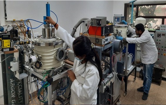
UHV Pulsed Laser Deposition System:
UHV pulsed laser deposition aka laser MBE system (SVTA, USA) is used to develop III-nitride epitaxial layers and nanostructures on various kinds of substrates including flexible metal foils at relatively lower temperatures as compared to conventional MOCVD and MBE techniques. In PLD process, a high energy laser beam is used to ablate the target material and the ablated species condense on a substrate to form thin film/nanostructures. A KrF excimer laser of 248 nm (Coherent) is employed for the target ablation. The system comprises of load lock/degaussing chamber, growth chamber, substrate/target heater, RGA, RF plasma cell and reflection high energy electron diffraction (RHEED) to assist III-Nitride growth and its in-situ monitoring.
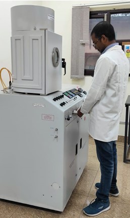
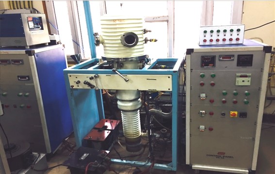
Thermal Evaporation System:
Thermal evaporation system is a simple thin film coating technique. The system (HHV, Bangalore) is used for the deposition of various metals thin films like Sn, Cu, Pd, etc. on different kinds of substrates. The equipment has substrate heater, thickness monitor, co-evaporation facility, etc. for the thin film deposition.
Thermal & E-beam Evaporation (Assembled):
Thermal & E-beam Evaporation system is used for the deposition of metal and metal oxide thin films.
Magnetron Sputtering System (Assembled):
Magnetron sputtering system is used for the deposition of various metal and metal oxide thin films using DC/RF electrical power. The system has substrate heater, which can be used up to 700 °C temperature.
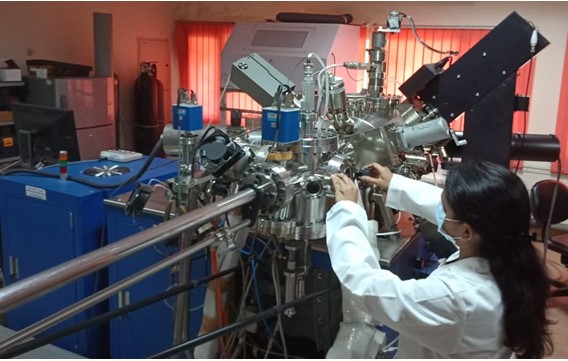
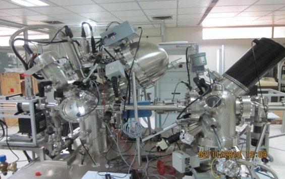
State-of-the-art Multi Techniques Surface Analysis System:
A multi-technique surface analysis system (Scienta Omicron, Germany) is equipped with X-ray (non-monochromatic& monochromatic source) & Ultraviolet (helium discharge lamp (He (I) & He(II)) photoemission spectroscopic. The system also equipped with a charge neutralization gun, sputter gun to eliminate the build-up charges and surface preparation before measurements, respectively. The system also contains microscopic techniques such as Scanning Tunneling Microscopy and Atomic Force Microscopy (RT to 100K). Besides this, Auger Electron spectroscopy, Scanning electron spectroscopy and Temperature Programmed Desorption technique are also available.
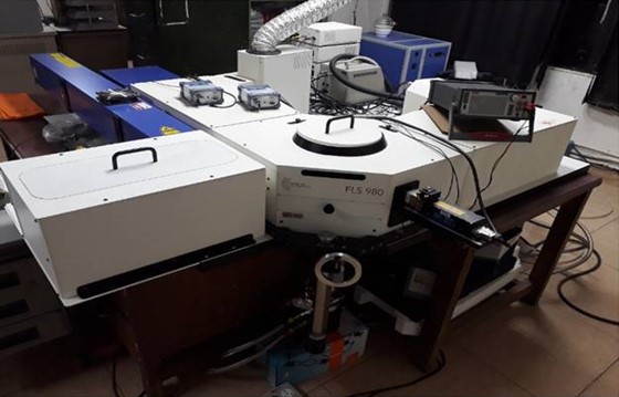
Photoluminescence (PL) Spectroscopy:
Photoluminescence is a nondestructive luminescence technique that can be used to probe the electronic structure of materials. In this method a laser source or a lamp with energy larger than the material band-gap is employed to excite electrons from valence band to conduction band. Electrons and holes recombine spontaneously either directly from conduction to valence band or involving different defect and excitonic levels in the band-gap. The emitted radiation is collimated, focused by lenses and directed to the monochromator that disperses the light into separate wavelengths. The dispersed light is then recorded by a CCD based camera detector and intensity vs wavelength plot can be viewed on a computer screen. The double monochromatic Room Temperature and Low temperature (upto 10 K) photoluminescence spectroscopy system (Edinburg, FLS 980 D2D2) is equipped with a continuous wave He-Cd laser (325 nm) and a Xenon lamp (200-1800 nm) as excitation sources with optical detection in the range between 230-1700 nm.
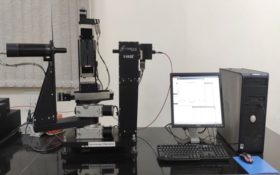
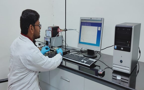
Spectroscopic Ellipsometer:
Spectroscopic Ellipsometer (J.A. Woollam, Model: V-VASE) is a non-destructive technique that can be used to measure the optical properties and thickness of thin films. In this method as elliptically polarized light falls on thin film sample and the reflected beam will be detected by a detector. The polarization of the incident beam will be disturbed by thin film and thus reflected beam carries the information regarding the thin film. The ellipsometer records the spectra of the variation of phase and the variation of the amplitude of the minor and major axes in terms of its ratio w.r.t wavelength, for different incident angles set. These spectra will be fitted theoretically by a range of expected n, k, d values using software adopting related theoretical models. Thus n, k, and d values are determined. Measurements can be made in the spectral range 200 – 1700 nm using Xenon lamp at variable angles of incidence.
Mini Spectrometer:
Mini spectrophotometer (Avantes, Model: AvaLight-DH-S-BAL) is used for the direct measurement of transmission, reflection, and absorption of the sample. Both thin films and liquid samples can be performed in the spectral range 200 – 1700 nm.
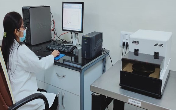
Stylus-based Surface Profiler:
Surface profiler (Ambios, Model: XP-200) is the direct measurement of thickness by step heights. This measure the step heights made over the surface when the surface is moved relative to the contact profilometer’s stylus.
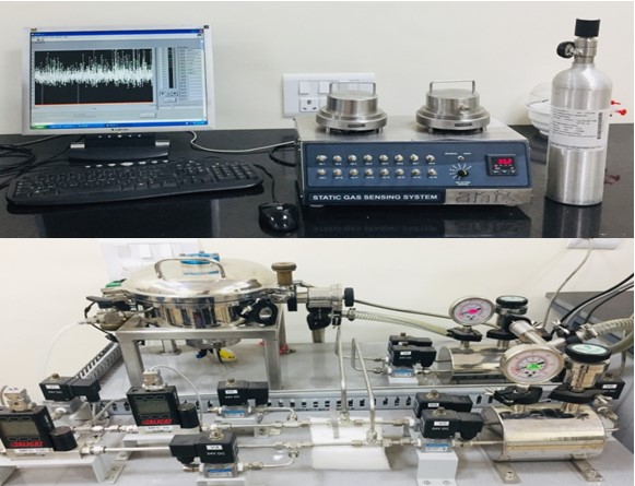
Gas Sensing System:
The group has custom designed static and dynamic gas sensing systems to test the performance of sensor elements for various pollutant gases. The sensor operating temperature can be varied from RT-500 oC.
Team
Dr. Govind
Chief Scientist
(DP Head & Group Leader)
Email: govind.nplindia@csir.res.in
+91-11-45609503, +91-9811930735
- Dr. M. Senthil Kumar
Sr. Principal Scientist
(Deputy DP Head)
Email: senthilmk.nplindia@csir.res.in
+91-11-45608609, +91-9717927838 - Dr. Preetam Singh
Sr. Principal Scientist
Email: singhp.nplindia@csir.res.in
+91-11-45608609,+91-9910025282 - Mr. Lalit Goswami
Technical Officer
Email: goswaml.nplindia@csir.res.in - Mr. Saket Vihari
Technician
Email: saketvihari.nplindia@csir.res.in